Laser-induced Chemical Vapor Deposition (LCVD)
LCVD is a method to deposit microscale solid patterns or three dimensional structures on the surface of a substrate by a localized, single step process. For the deposition of solid by LCVD, a focused laser beam irradiates on the surface of a substrate placed in a chamber filled with precursor gas to locally raise its surface temperature. Then, the precursor gas adsorbed on the heated substrate surface undergoes a thermally-induced chemical decomposition into solid deposit and gaseous byproducts (FIG. 1).
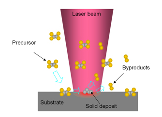
FIG. 1 Principle of LCVD
Because a focused laser beam is used for the substrate heating, the size of heated surface and thus the deposited pattern can be controlled to the order of a few micrometer. LCVD has been applied to the repair of electrical circuits (FIG. 2) or photolithographic mask patterns and also to the fabrication of three-dimensional micro structures. There exist two different types of LCVD, which are pyrolytic LCVD and photolytic LCVD. In Pyrolytic LCVD, an incident laser beam heats the substrate to a high temperature and precursor molecules adjacent to this hot surface are thermally decomposed to form a deposit. In photolytic LCVD, however, the incident laser energy is directly absorbed by the reaction gas to selectively excite precursor molecules. Generally, pyrolytic LCVD is more advantageous in achieving good electrical property, high deposition rate, high resolution, and high purity of a deposit than the photolytic LCVD except that the substrate temperature in pyrolytic LCVD is much higher than that in photolytic LCVD.
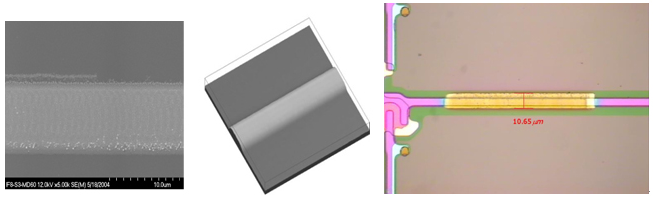
FIG. 2 Top view, left, and 3D profile, middle, of a tungsten line deposited on glass using LCVD and an application example of TFT-LCD circuit repair
Low electrical resistance is critical for semiconductor or electronics applications of LCVD, for example, TFT-LCD circuit repair. The electrical resistivity of LCVD-deposited tungsten lines depends upon the crystalline structure of the deposit which again is a function of deposition temperature. In our experiments, tungsten lines were deposited at temperatures below the softening point of LCD glass, 450℃-500℃. Despite the relatively low process temperature, it was possible to deposit tungsten lines with resistivity below 1 Ω-μm, the required level for an application to TFT-LCD circuit repair according to manufacturing standards (FIG. 3).
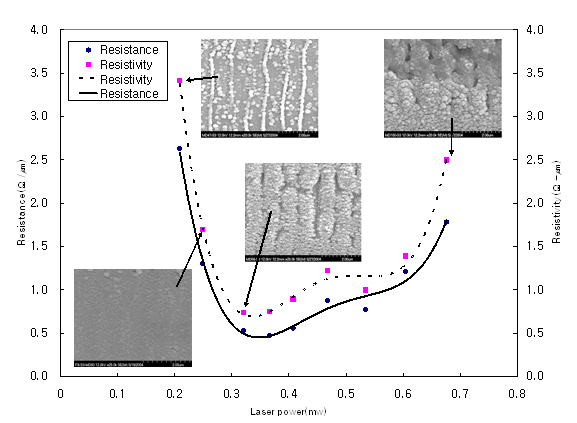
FIG. 3 Electrical resistivity of LCVD-deposited tungsten lines on TFT-LCD glass
Carbon nanomaterials
Carbon nanotube (CNT) is a cylindrical carbon structure with a diameter of on the order of a few nanometers (approximately 1/50,000th of the width of a human hair) and a length of up to several millimeters. CNTs are classified into single-walled nanotubes (SWNTs) for which the nanotube wall consists of only one-atom-thick graphite and multi-walled nanotubes (MWNTs) for which the nanotube wall consists of multiple layers (FIG. 1). CNTs have extremely high aspect ratio, exhibit extraordinary strength, are electronically semiconducting or metallic, and transfer heat very efficiently, which make them potentially useful in many areas. Examples of CNT applications under active research and development include special clothes or structures for space or sports, electrical circuits like terahertz source, supercapacitor, transistor, flexible display, field emission device, hydrogen storage, drug delivery, cancer treatment, solar cell, nanocircuits, nanomotors, fuelcells, etc (FIG. 2).
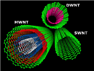
FIG. 1 Single-walled and multi-walled carbon nanotubes
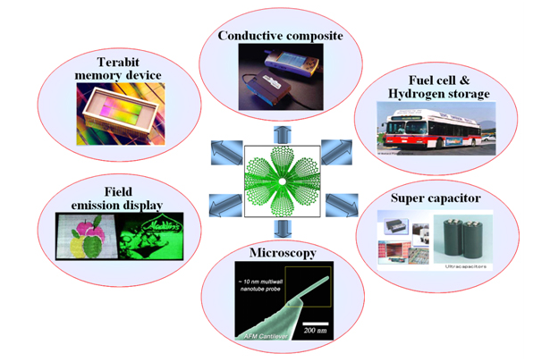
FIG.2 Potential applications of carbon nanotubes
Laser-induced CVD (LCVD) is an effective method for localized synthesis and direct writing of CNTs. In LCVD growth of CNTs, a focused laser beam directly irradiates the substrate, enabling the growth of CNTs with intrinsic benefits of localized, fast, and single-step processing.
In our laboratory, we developed a LCVD process in which a focused laser beam irradiates the backside of multiple catalyst layers deposited on a transparent substrate at room temperature (FIG. 3). By adopting the backside irradiation approach, contrary to the frontside irradiation utilized in most other researchers, we were able to grow SWCNTs and MWCNTs with much higher density than those reported in other studies. We have demonstrated the direct writing of MWCNT patterns of 8 mm in resolution with good uniformity (FIG. 4), the growth of pillar arrays of densely packed vertically aligned CNTs (FIG. 5), and high density SWCNT dots (FIG. 6). In this method, the growth of each CNT pattern is completed during a single irradiation period without preheating or annealing of the catalyst. These LCVD-produced CNTs and CNT patterns have high potential for micro and nano device fabrication.?
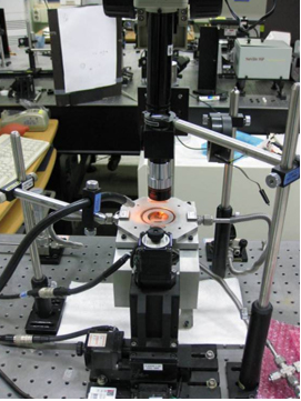
FIG. 3 Experimental set up for the growth of CNTs using LCVD
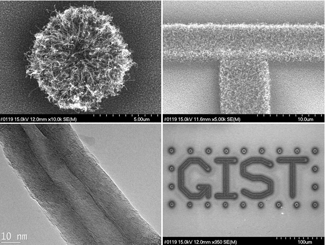
FIG. 4 MWCNT dot and line grown by LCVD and the direct-writing of ‘GIST’ using CNT patterns
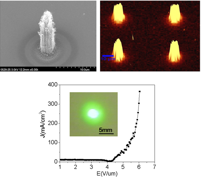
FIG. 5 Vertically-aligned CNTs grown by LCVD, top left, and confocal Raman spectrum image of 2x2 array. The graph at the bottom shows the field emission characteristics of a 10x10 array.
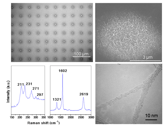
FIG. 6 Single-walled carbon nanotubes grown by LCVD
Carbon-encapsulated magnetic nanoparticles (CEMNPs) have many applications in diverse fields such as ferrofluids, contrast enhancement in magnetic resonance imaging, magnetic data storage, xerography, and magnetic carriers for drug targeting, etc. The encapsulation of magnetic nanoparticles with carbon provides a protective shell that improves chemical stability of metal nanoparticles, whereas the use of pure magnetic metal nanoparticles such as iron (Fe), nickel (Ni), and cobalt (Co) results in inherent instabilities such as oxidation in air, dissolution in acid, and easy agglomeration which limits the potential of these particles for use in industrial or scientific applications. Fe, Ni, and Co are important materials in nanoparticle study due to their ferromagnetic properties and their unique catalyzing ability to transform amorphous carbon into graphitic carbon at sufficiently high temperatures.
In our laboratory, we developed a photochemical method for the synthesis of CEMNPs under the conditions of room temperature and atmospheric pressure. In this method, CEMNPs are produced by the pulsed laser irradiation of a solution (PLIS) prepared by dissolving different metalocenes in xylene in which the dissolved metalocenes form the magnetic core and xylene is the carbon source for the formation of the graphitic shell. The CEMNPs synthesized by the PLIS method have well-ordered graphitic shells and thus a strong resistance to environmental degradation effects such as oxidation in air and dissolution in acid, and also show soft ferromagnetic properties. Since the PLIS method is simple and can be operated under ambient conditions, it is considered that CEMNP synthesis can be scaled up easily with a high power laser system and particles of uniform size can be produced.
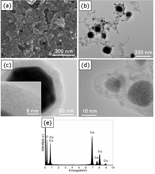
FIG. 7 (a) SEM and (b) low-magnification TEM images of the Co-C nanoparticles. High resolution TEM images of (c) large (200 nm) and (d) small (10 nm) Co-C nanoparticles with graphitic layers: the inset shows a magnified view of the outer shell for which an inter-planar distance of 0.34 nm is estimated. (e) Representative EDX signal of Co-C nanoparticles.
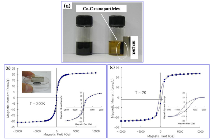
FIG. 8 (a) Photograph of the Co-C nanoparticles dispersed in xylene (left) and their response to a magnet (right). (b) Magnetization curve of the Co-C nanoparticles at room temperature (300 K): the left inset shows the dried Co-C nanoparticles in a gelatin capsule to measure the magnetic properties, and the right inset shows a magnified view of the low magnetic field data. (c) The magnetization curve of Co-C nanoparticles at low temperature (2 K).